Tutorials and Tools
Transfer of graphene films grown by CVD to arbitrary substrates
Chemical vapor deposition (CVD) proved to be a successful route for synthesis of large area graphene films on transition metals. However, for various applications, the obtained graphene whether single layer (SLG) as in the case of growth on copper foils or few layers (FLG) as in the case of growth on nickel thin films requires transfer to a destination substrate for device fabrication. The main criteria for a successful transfer process is that it should result in smooth defect-free graphene and be compatible with a wide range of target substrates. [1] However, it is believed that during the transfer process a significant degradation of the quality of CVD graphene occurs due to ripping, folding or tearing up the sheet. [1] Thus, significant effort has been put by the scientific community towards optimizing existing transfer techniques and developing new ones with the aim of maintaining the quality of the as grown samples.
The basic principle underlying all the transfer methods of CVD graphene is to employ a support layer placed on top of the graphene layers to protect them and provide a mechanical support during the subsequent transfer steps. Then chemical etching of the underlying metal film is carried out. After the etching process, the graphene/support bilayer is transferred to the destination substrate followed by the removal of the support layer. Depending on the support layer used, transfer methods are generally classified as carrier or stamp transfer methods. [2] Carrier transfer methods utilize a support layer that adheres strongly to graphene, and requires aggressive chemical or annealing treatments to be removed. Examples for carrier transfer processes include the use of popular Poly (methyl methacrylate) PMMA film or thermal release tapes. The main issue with such methods is that graphene is typically left with residues of the support layer that are difficult to be completely removed, affecting its electrical properties and surface roughness which influences the subsequent device fabrication. In addition, chemical and thermal treatments used to remove the support layer are usually not compatible with device fabrication as it would adversely affect other device components. Stamp transfer methods utilize an elastomeric support layer that picks up the graphene layer and stamps it onto the destination substrate. These methods typically utilize Polydimethylsiloxane PDMS as the support layer, which has a weak adhesion to most materials. Removing the stamp layer relies on the thermodynamics of the adhesion forces between the stamp and the graphene from one side and the graphene and the destination substrate from the other side. The stamp support layer is removed simply via mechanical peeling, which would leave the graphene film intact to the destination substrate leaving no residues on the surface. However, mechanical stresses during the release step can introduce cracks to the graphene. PMMA mediated transfer has been successfully demonstrated to transfer carbon nanotube and create various nanostructures showing high efficiency and universality.[3] It has been extended to transfer CVD graphene from the catalyst metal to any targeted substrate, [4, 5] by spin coating a thick layer on the polymer, followed by chemical etching of the metal leaving the PMMA/graphene floating on the etchant. After washing with DI water, it is simply scooped on the target substrate forming PMMA/graphene/target substrate structure after which the PMMA is washed away in acetone leaving graphene on the substrate. However, due to the covalent bonding between PMMA and graphene, [1] the washing step always leaves PMMA residues on the surface of graphene which increases its roughness and introduce a non-intentional p-doping. To further clean the surface of graphene from PMMA residues, the samples are further annealed in vacuum [6] (42) or H2/Ar mixture [7] at 300 ᵒC, which greatly enhances the electrical properties and smoothness of obtained graphene. A further improvement to the PMMA transfer method that proved to enhance the quality of transferred graphene was introduce by Ruoff et al, [4] where a second layer of PMMA was placed on the PMMA/Graphene after scooping to the target substrate. The second layer is believed to partially dissolve the first one, and hence allow the graphene to release any prior rigidly held folds and ripples, and hence provide a better contact to the target substrate. Stamp transfer methods most commonly utilize PDMS layer to mechanically support graphene, a concept borrowed from soft-lithography, where microstructure can be replicated using pre-patterned elastomer masks. The PDMS stamp is attached to the graphene sample, followed by chemical etching on the underlying metal catalyst, the PDMS/Graphene can be left off using a tweezer, washed and dried and then stamped on the target substrate. This is to be contrasted the scooping step in PMMA transfer method, which is advantageous for target substrates or devices that are sensitive to moisture and other solvents. The stamp can be then peeled off leaving the graphene on the substrate. PDMS is durable, unreactive and attaches to the graphene via weak Van der Waals interactions, which lead to a clean and residue free graphene surface. This allows spontaneous graphene detachment to the destination substrate; provided that the graphene film has a conformal attachment to the PDMS stamp and the target substrate. This method has been demonstrated to transfer either continuous or patterned SLG [8] and FLG [9] graphene on SiO2/Si. The only requirement for a successful stamp transfer process is that the work of adhesion – defined as the energy needed to separate two solids at the interface into their respective free surfaces – between the graphene and PDMS (source) to be lower than that between the graphene and the target substrate (destination). The work of adhesion is a function of the surface energy of the materials in contact; hence this equation can be represented as a comparison between the surface energy of the PDMS and that of the target substrate. The former exhibits a surface energy of 20 mJ/m2, which is typically lower than most materials. [10] 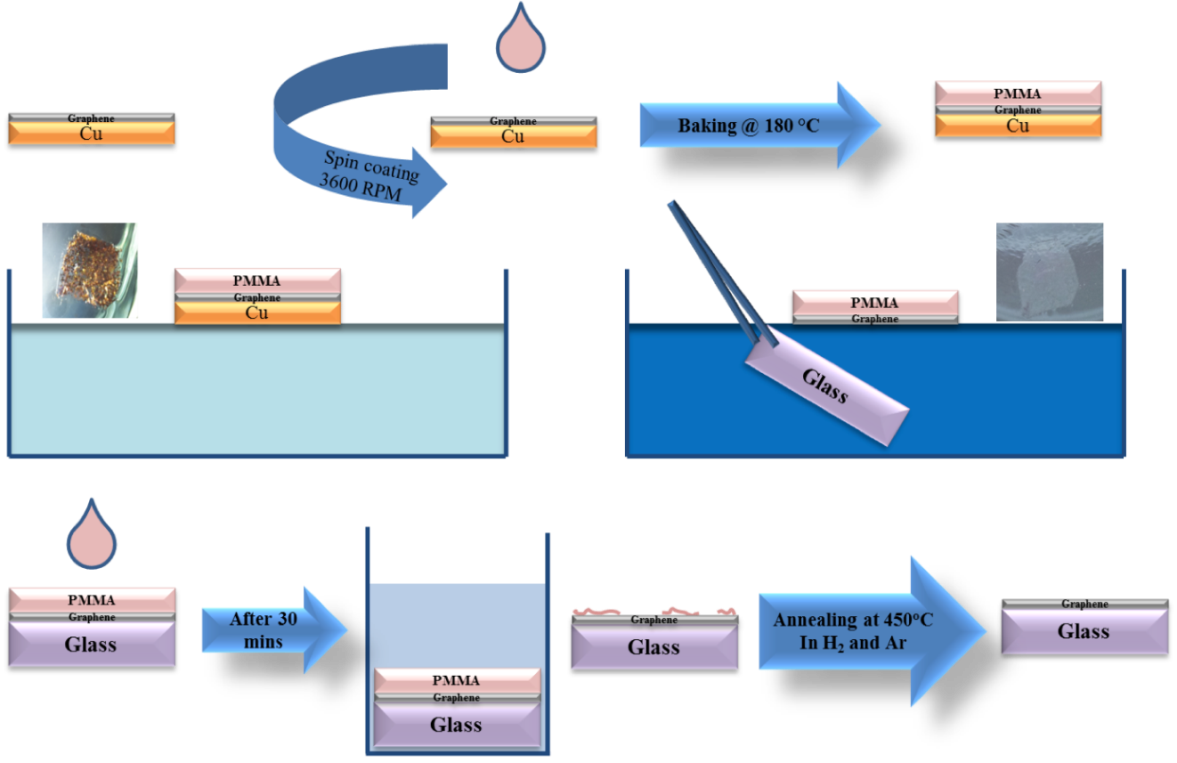
Figure 1: PMMA carrier transfer method of graphene from copper foil to target substrate.
Figure 1 illustrates the general procedure for the transfer of CVD graphene. I will share in the following the standard operating procedure for carrier transfer methods that I have optimized and used during my PhD research.
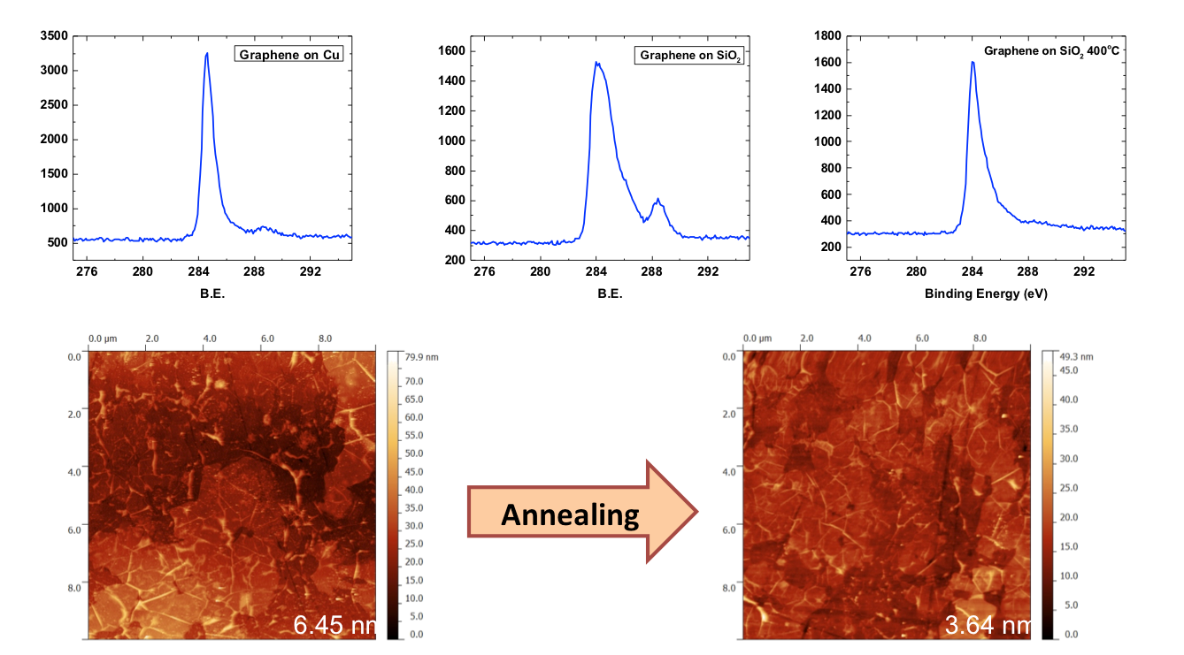
Figure 2: Effect on the annealing process on transferred graphene samples. High resolution C 1s XPS peaks on copper, transferred to SiO2 and annealed at 400 °C. AFM of FLG graphene with the RMS roughness before and after annealing.
To overcome the disadvantages of PMMA transfer, as well as eliminating the need of the annealing step, dry transfer using PDMS stamp was also routinely conducted during my PhD work.
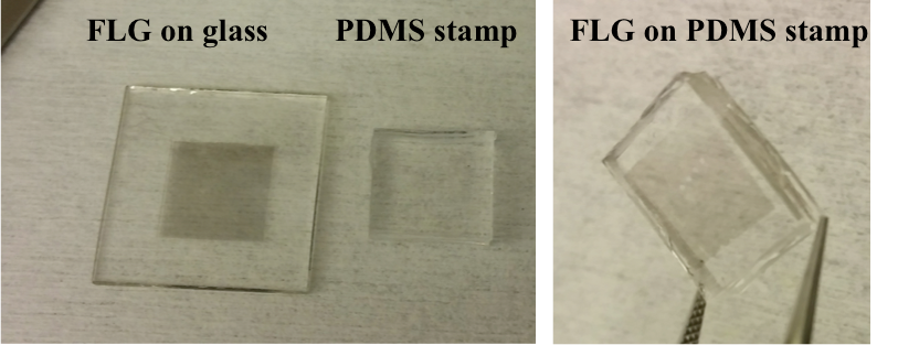
Figure 3: Demonstration of PDMS stamping method. PDMS stamp is pressed on top of FLG/Ni/SiO2, followed by chemical etching of the nickel. The resulting FLG on PDMS can ideally be laminated on any targeted substrate (on glass in this figure)
References:
[1] J. Kang, D. Shin, S. Bae, B. H. Hong, Nanoscale 2012, 4, 5527. [2] J.-Y. Choi, Nat. Nanotechnol. 2013, 8, 311. [3] L. Jiao, B. Fan, X. Xian, Z. Wu, J. Zhang, Z. Liu, J. Am. Chem. Soc. 2008, 130, 12612. [4] X. Li, W. Cai, J. An, S. Kim, J. Nah, D. Yang, R. Piner, A. Velamakanni, I. Jung, E. Tutuc, S. K. Banerjee, L. Colombo, R. S. Ruoff, Science 2009, 324, 1312. [5] A. Reina, X. Jia, J. Ho, D. Nezich, H. Son, V. Bulovic, M. S. Dresselhaus, J. Kong, Nano Lett. 2009, 9, 30. [6] A. Pirkle, J. Chan, A. Venugopal, D. Hinojos, C. W. Magnuson, S. McDonnell, L. Colombo, E. M. Vogel, R. S. Ruoff, R. M. Wallace, Appl. Phys. Lett. 2011, 99, 122108. [7] Y.-C. Lin, C.-C. Lu, C.-H. Yeh, C. Jin, K. Suenaga, P.-W. Chiu, Nano Lett. 2012, 12, 414. [8] S. J. Kang, B. Kim, K. S. Kim, Y. Zhao, Z. Chen, G. H. Lee, J. Hone, P. Kim, C. Nuckolls, Adv. Mater. 2011, 23, 3531. [9] K. S. Kim, Y. Zhao, H. Jang, S. Y. Lee, J. M. Kim, K. S. Kim, J.-H. Ahn, P. Kim, J.-Y. Choi, B. H. Hong, Nature 2009, 457, 706. [10] J. Song, F.-Y. Kam, R.-Q. Png, W.-L. Seah, J.-M. Zhuo, G.-K. Lim, P. K. H. Ho, L.-L. Chua, Nat. Nanotechnol. 2013, 8, 356. |
Contents:
|
