Characterization of the charge carriers in molecularly doped organic semiconductors using optical spectroscopy and Raman spectroscopy
Motivation
Organic semiconductors (OSC) have emerged as an important class of materials for electronic applications. Their inherent chemical versatility, mechanical flexibility and ability to be processed from solutions have put them as a front-runner candidate towards applications where flexible devices and cost-effective large scale production are desired. However, due to the intrinsic low charge carrier density in OSCs, additional strategies to improve their electrical transport properties were investigated and has been the focus of the research community for decades.
A successful strategy that has been developed and intensely researched is molecular doping of OSC. Molecular doping is defined as the process of adding a small number of molecules (dopants) into a matrix of an OSC (host). Such a process – when carried out with a proper choice of dopant and host – results in increasing the charge carrier density which in turn enhances the electrical conductivity of OSC, as well as, tuning their energy levels which improves the charge injection and collections at interfaces in electronic devices.
A feature of electrical charges in OSC is that they couple with the molecular entity of the OSC. This means that the introduced charges by doping are accompanied by a geometrical distortion in OSC, which localized the charges over a certain part of the OSC (a number of monomeric units in the polymer). These charges are known as either polarons or bipolarons depending on the number of charges coupled with the geometric distortion (polymer segment).
The prevalent importance of identifying, quantifying and understanding the characteristics of the charge carriers in OSC has led to the reliance on several spectroscopic techniques to uncover and optimize the doping process, such as electron paramagnetic resonance spectroscopy (EPR), optical spectroscopy and vibrational spectroscopy. While EPR is a conclusive technique to differentiate polarons and bipolarons, it is a specialized technique the requires relatively cumbersome sample preparation and sophisticated data measurements and analysis, as compared to optical spectroscopy and Raman spectroscopy. Utilizing the versatility and simplicity of optical and vibrational spectroscopy to study the type and characteristics of charge carriers in OSC is highly beneficial for the scientific community towards the investigation of molecularly doped polymers.
|
Approach
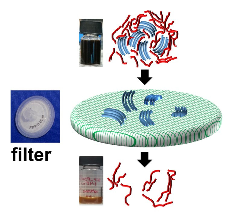
During my postdoctoral research assignment at Humboldt University in Berlin, I focused on investigating the nature of doping introduced charge carriers in polymers using UV-Vis-NIR optical spectroscopy and Raman spectroscopy. Optical spectroscopy is a highly suitable technique to study polarons and bipolarons in polymers since their formation is accompanied by the introduction of new localized electronic states in the bandgap of the polymer, which are involved in the electronic transitions directly detected by optical spectroscopy. On the other hand, Raman spectroscopy, which detects the vibrational modes along the polymer chain, is a facile and sensitive tool to probe the changes in the geometry of the polymer upon the introduction of changes due to the strong electron-vibron coupling in OSC. Identification of the optical signatures of polarons on isolated chains and aggregates in molecularly doped P3HT:
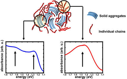
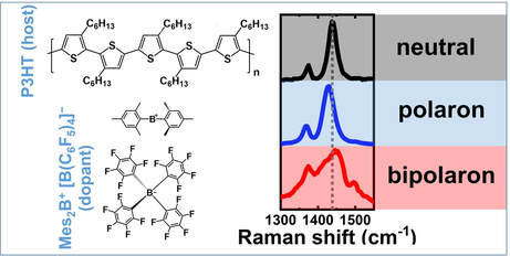
Identification of the Raman signature of polarons and bipolarons in molecularly doped P3HT:
|
Modulation of the electronic, optical and transport properties of graphene via chemical doping: Towards application as a transparent conductive electrodes
|
Motivation:
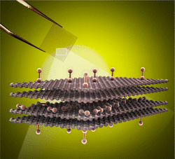
Graphene has emerged as a strong candidate as a transparent conductive electrodes (TCE) as a potential replacement for the popular Indium Tin oxide (ITO). This is due to the unique fundamental electronic, optical, mechanical and chemical properties of graphene. However, large scale production routes of graphene (currently most popular it the Chemical Vapor Deposition "CVD") is poly-crystalline and defective, resulting in a lower conductivity as compared to higher quality graphene. Hence to capture the advantage of the large-scale processability of CVD graphene, chemical doping can significantly reduce its sheet resistance, in addition to largely modifying its work function which enables universality of using graphene either as a low work function cathode or a high work function anode in optoelectronic applications. Approach:
|
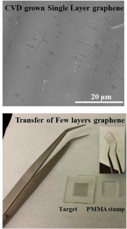
Chemical Vapor Deposition (CVD) of Graphene - optimization and clean transfer
|
Motivation:
Chemical vapor deposition (CVD) is currently the most promising route towards large-scale production of graphene, especially with very recent reports on the roll-to-roll adaptation of both the synthesis and transfer process. The properties and uniformity of CVD graphene are largely influence by the conditions using during it preparation and to a large extent by the transfer process. A proper optimization of both of these processes is an essential step for any laboratory working on graphene. Approach:
|
Structural and Morphological changes to CVD graphene upon exposure to Oxygen plasma
Motivation:
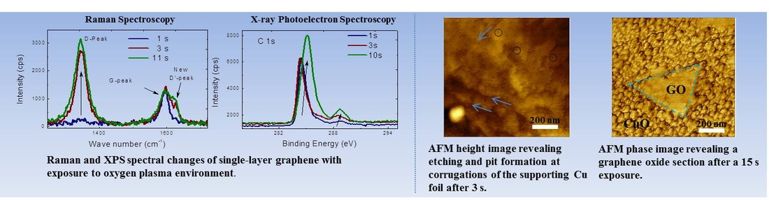
Graphene oxide has emerged as a solution-processed route to produce graphene thin films. However, to be the conductivity of graphene oxide films are significantly higher than those of synthesized from CVD, and hence a reduction process is required to restore the properties of pristine graphene. However, it has been challenging to restore the structure of pristine graphene and achieve full removal of the oxide species. A better understanding of the structural, morphological and chemical evolution of the oxide species on graphene can aid in developing better strategies for reducing graphene oxide towards pristine graphene.
Approach:
- Controllable oxidation of an initially high quality pristine graphene (CVD Single Layer Graphene).
- Chemical and Structural analysis at each oxidation stage via XPS and Raman spectroscopy
- Monitoring the morphological changes via AFM.